(According to an article published in Hobbytronic No. 10, 14 and 17 by E.Deret)

Hourly, daily and weekly Scheduler based on the MC68705P3 microcontroller
(According to an article published in Hobbytronic No. 10, 14 and 17 by E.Deret)![]()
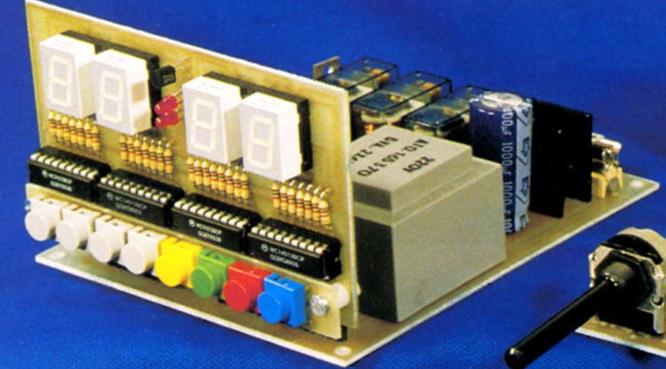


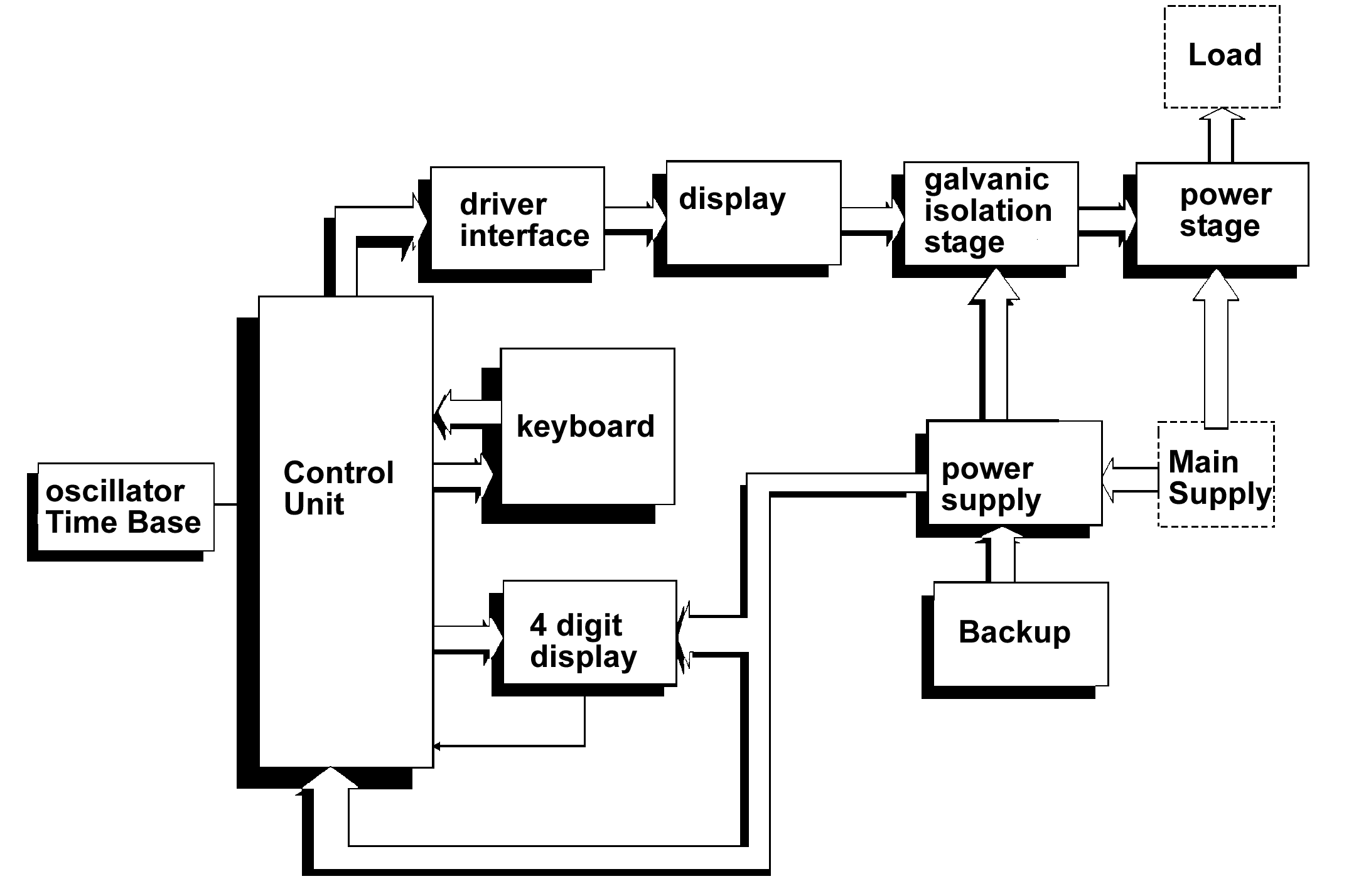
This timer is used to control the starting and stopping of 4 devices connected to the mains. The information display can be performed equally on 7-segment display or LCD display 4 digit half. Recognition of the type of display is automatic and the program automatically adapts itself to pilot it.
The data entry is done from a 8 keys keyboard.
This achievement is divided into 3 modules (CPU, display and keyboard).
Memory of the CPU was shared in order to contain up to 30 commands commissioning and decommissioning.
Alongside these programmed functions, there is the possibility of being able to start forced each output.
The microcontroller is clocked by a 3.2768 MHz crystal.
The management unit and control manages the scanning keypad with 8 keys, it is also responsible for updating the value to be edited on the 4-digit display. These four digits can display in 24 hour format which is not possible with a three-digit display and a half (size limited to 12 hours). Because of the possibility of receiving two types of displays, information is returned to the display part to enable the UGC to know which one is used (LED or LCD). Finally, the UGC driver control interface that controls the outputs.
The supply side, nothing special to report except that the presence of a backup story that allows the UGC to continue to function in case of power failure. This attack also saved power displays 4 digits in the case of the LCD display (very low consumption). For LED displays, this is the normal supply is used.
The control interface portion will simultaneously control the visualization of the activated output stage and the electrical isolation. End of the chain is the power stage that will power the load activated.
Analysis of the assembly:
the circuit arrangement has four subsets which are:
- The CPU card that supports any microcontroller and the interface part and power supply.
- Keyboard layout: this is by far the easiest. It is thanks to her that perform order entry.
- The display board LED or LCD card: the last two provide the information visualization in use
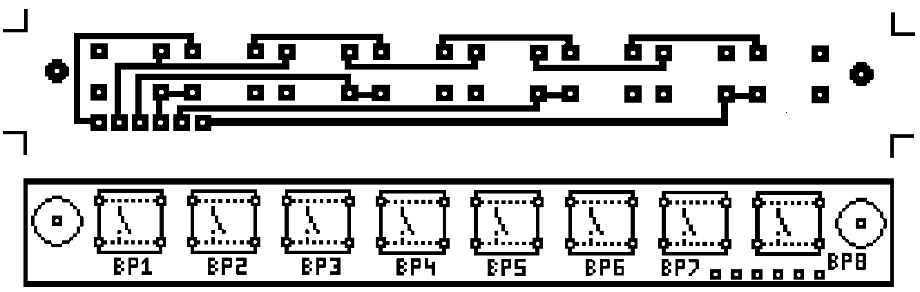
Keyboard layout:

8 pushbuttons matrixed into 2 rows / 4 columns. The association with the rest
of the assembly is by a 6-pin connector.
Two possible solutions: either PA2 PA5 lines are configured output lines PA6 and PA7 configured as input, or vice versa.
The first solution requires four readings of 2 bits in the clear reading of
BP1 and BP2 and BP3 reading and then reading BP4 BP7 and BP8 and finally reading
BP5 and BP6. The other solution comprises two readings of 4 bits, ie reading
BP2, BP4, BP8, and then reading BP6 BP1, BP3, BP7 and PB5. The 68705 is not
among the fastest microcontrollers is of course the second solution will be
used, which uses only two read cycles.
Each of the lines are drawn PA2 PA5 to ground by a resistor network. This offset
components keeps the entire assembly consistent behavior even in the absence
of a keyboard (no risk shuffle).
Reading lines PA2 PA5 receives a permanent low state when no key is pressed.
This is a high state which must be applied to PA7 PA6 and to scan playback.
Miniature push the ITT KSA have 5 pins. The four end are connected together in pairs. This structure is equivalent to many straps. This simplifies the PCB. A fifth tab located (in the axis of the pusher) can shield the housing. It is not used on this assembly. It may be cut before insertion.
The LCD
4 decoders BCD / 7 segment 4543 CMOS fly each digit of the display.
The value to be displayed is passed to the decoder BCD form. It is on the inputs ABCD it is applied. But looking more closely at the diagram, we see that the binding of these four input lines is done in the most complete disorder between 4 decoders (A connected D, next door, connected with B C). In order to have a PCB as small as possible and the opportunity to remove eight straps.

ABCD inputs are controlled by lines PB2, PB3, PB4 and PB5 the microcontroller.
Line PB0 is used to select the display dozens of hours, the line PB1 selects
the units of hours, tens of minutes PB6 PB7 and units of minutes.
Why legs PB1, PB6 and PB7 have no resistance as the line PB0 +? All four are
sure to select a decoder? Another handy trick that saves the input / output
of a microcontroller. In normal use, all lines of port B must be configured
to ensure the output display. Nothing prevents the input set in the initialization
phase. At this stage, it is possible to read a configuration state. The resistor
R1 on this card is certainly the most important. LED on the display board, the
same resistor is connected to ground. It is what allows us to know what type
of display is mounted on the realization. The mention on either cards or lead
to the destruction of the LCD (No signal BACKPLANE) or an incoherent display
on the LED board.
At boot time, the microcontroller sees a high state on this line and immediately knows it must run a LCD type display.
Here is the truth table of the decoder BCD / 7 segment used:

On port A, both lines are used. Line PA1 pilot the two central points. They serve as indicators of seconds.
PA0 line generates the signal BACKPLANE see ***
The decoders type CMOS4543 have any internal network exclusive OR gate needed to control an LCD display. The signal is therefore BACKPLANE applied thereon.
The rest of the lines of port A is used for the keyboard.
The map display can be used as a card holder for keymap (keyboard alignment relative to the display). It must therefore contain a reference connector.
The power of the LCD map is provided by the line of 5Volts saved. This allows for permanent display even in case of power failure.

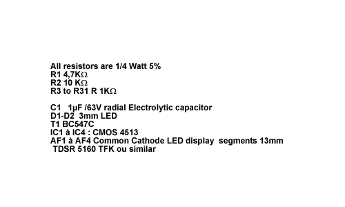
List of components:
R1 4.7K 1/4 Watt
IC1-IC4 CMOS 4543
LCD Display 4 digits 1/2
Realization
Some precautions must be taken to achieve this map. First, start by installing the four straps.
The role of Straps S3 and S4 is a bit unusual and has not been addressed in the detail drawing. Reason! Typically, LCDs have more segments than there really needs. Or to prevent accidental ignition of these, it is advisable to connect the signal BACKPLANE. It is realized that these two straps.
Extra precaution! LCD displays are components that do not support the heat and especially that of a soldering iron. It is therefore wise to their integration into strips support.
4543 Pinout CMOS and LCD:


The LED display
The detail drawing
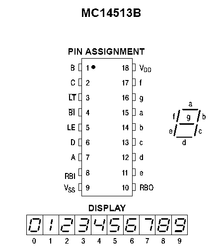
The seven-segment decoder used previously was not used for this card because it is not able to provide enough current to light the LED. It is therefore to a CMOS 4513 that was chosen.
This component has been selected specifically for the font that is capable of providing (presence of the bar on the upper and lower 6 and 9
Here is the truth table of CMOS4513:

This component is equipped with an erasure of the display (Blanking). It has not been used for two reasons: The first is that the 68705P3 has only 20 lines of input / output and they are all already in use. The second is that the "blanking" can also be obtained by sending the decoder non-decimal value (operation identical to that of the LCD). It is this principle that is used on the two cards.)
Microcontroller side, the scheme has little difference (Mixture data lines A, B, C and D PB2, PB3, PB4 and PB5; selection decoders on PB0, PB1, PB6 and PB7). R1 is the resistance this time grounded which confirms the explanation given on the recognition of the type of card. Note that the two cards that resistance is wired in the sense that it affects the least storage of the data (storage control signal reversed on both decoders).
The differences are only PA0 and PA1 lines. PA0 line (signal on the backplane board LCD) is not used to it (which is quite normal). PA1 command line still display for two seconds. Resistor R2 limits the base current in transistor T1. The display is made on the LEDs D1 and D2, whose current is limited by the resistor R17.
Side 7-segment display, it is common cathode type displays. The current flowing through them is limited to 5mA for reasons of consumption and dissipation. This limitation is produced by the resistors R3 to R16 and R18 to R31.
This solution was considered more interesting than the realization of multiplexing that makes no difference in brightness.
Like all cathodes are connected to ground, the power supply operates directly under 5 volts. This is an unsaved 5V is used. There is necessarily display disappears when power outage. The capacitor C1 is made necessary to avoid problems caused by the current on important calls displays.

List of components
Realization
The installation displays can be made on supports 24 blades with 4 legs have been removed from power.
LEDs used to display the second must be aligned with the display in order to have all light sources in the same plane.
Pinout CMOS 4513

Pinout TDSR5160
Pinout BC547C
The CPU
The detail drawing

The centerpiece of this card is made by the microcontroller.
Lines of Port A and Port B on the lead connector CN1 to act as liaison with the maps display and keyboard. The resistance bridge PR1 to define a precise when no key is pressed.
C4 is reset capability (recall load resistor is integrated in the microcontroller). The capacitor C3 is used for decoupling and R1 sets a constant state of the interrupt input.
Part oscillator (Q1, C2) is classic. A particular point to note however is: quartz crystal is 3.2768 MHz. This value out of the ordinary was not chosen at random. This is an integer power of 2 (32768 = 2 ^ 15). This particular point can work directly with the divider for the timer time base of 1/100th of a second. From that moment, the clock accuracy is only a function of the precision of quartz. This little trick is commonly used in all circuits clocks.
Part supply: transformer provides a voltage of 2x6Volts alternative. This voltage undergoes a wave rectification by the bridge D3-D6 and filtered by capacitor C5. RG3 controller provides a voltage of 12 Volts, which will power the power control part.
RG2 regulator lowers the voltage to 5 volts to power the card LED display. It can not be mounted when the card is the card LCD display. The filter capacitor is transferred to the LED board.
The diodes D1 and D2 are used to switch the power on the battery power failure. The regulator RG1 also lowers the voltage to 5 volts. She is going to power the CPU and LCD display. It is therefore saved by the battery. Consumption on this line is of the order of 80 to 100 mA. So make sure to always have a battery in perfect condition. Capacitor C1 filters the resulting voltage.
The power: Lines used to go and order the 4 outputs are lines of port C to be all configured output. The power interface is formed by the ULN2003 (IC2)
The power control part. Either by an opto-triac or a relay.
In the case of mounting opto-triac, the resistor R3 limits the current flowing
through the LED of the optical coupler. In series we find the LED indicator
of activation of the output (D7 to D10). Sector side, we find the traditional
assembly triac driven by R4 and R5 with R6-suppressor network C7.
In the circuit relay, resistor R2 limits the current through the LED for commissioning. Sector side orders can be taken both on contact work on the NC contact). A small novelty is the possibility to recover the output contact (RTC). This solution allows any kind of wiring devices on the output.
List of components

(*) Relay JW1FSN-DC12V JW relay. Compact PC board power relay. 1 form Matsushita / Panasonic
Realization
The realization of this card requires a number of precautions.
Firstly it is a mount that found connected to mains. Therefore comply with all the rules on this kind of wiring (quality control of welds, no short circuit, etc.)..
The big problem is first based on the choice of the configuration of the power stage. This choice will depend on the nature of the components to be wired.
There are 5 different possible cases for this assembly:
Case 1: This is where the relay is used as a dry contact. The assembly therefore comprise apart over the resistance R2 limiting the current in the LED.
Case 2: This is the case where mixed contacts simultaneously work and rest are used. Both networks noise R6 and R7-C7-C8, plus R2 should be added to the relay. In this case the point of common contact to be connected to the mains supply line by a solder bridge.
Case 3: This is where only the contact work is used. The assembly is identical to the case that the network 2 except R7 is not C8-mounting.
Case 4: This is the case or break contact alone is used. The assembly is identical to the case that the network 2 except R6-C7 must not be mounted.
Case 5: This case is the use of a mounting an opto-triac. The components to be mounted are: the opto-triac IC4, resistors R3 to R6, the capacitor C7 and the triac TR. As for case 2, a solder bridge must be made between the power line and the arrival runway of the triac.
Each case of implantation is shown in figure below

The PCB has been designed to receive the three types of transformer.
1.8 VA for the model, there is no particular trap. Against by the other two, a little precaution must be taken. A jumper must be wired to allow connection to the second side. (For Model 3.5 VA) or the link between the two secondaries (for model 5VA). So watch for the positioning of the strap, as in the case of error, it is the transformer that smokes ...
The resistance bridge has 6 legs. But only 5 are used. Care should be taken to fold the second (starting point) before inserting.


ULN2003 ***
MOC3041 ***
7805, 7812, 78L05 ***
The final assembly
You now have three hands modules (CPU, display and keyboard) that will have all together.
Where the solutions are many and varied
On our prototype, the keyboard was mounted directly on the map display using 2 spacers 5mm height and nylon nuts. The connection between the two cards was performed with tails components.
The link unit displays - is made through connectors (female Human wide on the CPU and bent the male displays).
The use of rigid monofilament ribbon cable with 2.54 is perfectly conceivable.
This provides greater flexibility canning.
Beware though, the connection between the cards should be as short as possible to avoid potential disruption of electrical signals.
The details of the connector is provided on the detail drawing.

Use
The entire explanations focus on its use in weekly mode. Daily and hourly patterns are only special cases. Their use is an adaptation of the general explanation will be given in due course.
Order entry occurs through 8 keys whose role changes from one function to another. To be able to navigate more easily, a small diagram showing the role of each key will accompany each of the modes in which may be mounting. If nothing is specified for a key is that it is not used in this mode.
Representations of dials accompany each step. Digits crowned simulate blinking while those hollowed simulate the rapidly changing digits.

At power up, the program initializes all its ports, memory and comes to determine the nature of the display system. Once all these steps internal investigations, we obtain the phase of the clock time. The display flashes and the time is initialized at 00:00.
0:00

The adjustment is made by switching to setting the time. No other function can be called as this phase has not been completed.
The clock
It is in this mode that is most of the time, the editing.
The screen looks like this:

The digits are fixed and two central points flash to the rhythm of seconds. two digits left of the viewing hours while those on the right visualize minutes.
In the previous example it is 24:34.
In this state the following key functions fulfilled

- Access output x: These four buttons are used to enter programming phase or activation of the corresponding output.
- Second: this button will display the value of seconds. The left digit will be deleted. Those on the right evolves in seconds. The screen takes the following form
So we can say that it is 12 hours 34 minutes and 56 seconds. In releasing the button, the display shows the hours.
- Day Use this button to display the value of the current day. The digits to the left are also deleted. The screen takes the following form:
This is the third day of the week. The days are treated relative (In fact, the screen does not display clear day value).
- Setting the time: this button will switch to update the time. Once in this mode, the keys are a different meaning.
Upon arrival in this mode, the screen takes the following form:
The left digit will flash signaling that it is time that the game will be changed. The advance of the counter is done by pressing the PLUS. A short press to advance a single step.
In this case the display digits of the hour is flashing.

If instead of a short press is a permanent support which is applied to the PLUS button, the flashing stops and the digits are incremented automatically one step every half second.
Releasing the button PLUS remember the flashing display.
In some cases, it may be faster to adjust by starting a timer. This case is obtained by pressing the reset button.

When setting the time part is done, the validation is done by pressing NEXT. The system then automatically switches to set the minutes.
These are the digits for the minutes flash that now.

The principle of the minute setting is identical to that for hours. PLUS keys, reset, and have the same role SUITE but transposed to minutes.
When the minute setting is completed and the validation was made by the CONTINUE
key, the system will automatically adjust the date.
The two digits on the left and the two are off right flash.

Just like minutes, PLUS, SUITE reset and have the same functions.
As already mentioned, the seizure of the day takes place on. Its value can vary from 01 to 07. As the assembly is not possible to know the schedule, both assign the value 01 to Monday. This little rule simplify the programming part of the outputs.

It is during this phase that will define the mode of operation of the assembly. In fact, the day value can vary from 01 to 07. Regulars of digital processing have already seen that there is an available value is 00. It is possible to assign this value to the day. From this point, the system operates in weekly.
All programming already in memory will automatically run every day.
This bracket is closed, let the course of setting the time. When pressing the CONTINUE key, the seconds are initialized to zero, thus setting the second around the clock. The display returns to the one given at the beginning of this chapter
Throughout this phase of the time, it was found that points to visualize the second still flashing. This landmark is important to know in which phase adjustment is mounting.
Output management
Whatever the phase in which the system is located, control and output activation is permanent (except in the initial phase for the first time at a time when no cycle is still programmed).
Access to functions on an output is obtained by pressing the key corresponding to this output (output 1 Access Access to exit 4).
From this moment on (release key consideration), the keyboard is defined as follows
For the display section, two cases are considered: either the memory is blank
programming the output in question, or that the memory has at least one programming
this output.
Memory is blank, two new cases may arise:

- Either it is space in memory and the display looks like the following:

The display is blank with two central points well lit to indicate that the circuit
is energized. This screen indicates that there is a way to add a program cycle.
- Either there is more space in memory and takes screen looks like this:
All digits are lit to indicate that there is more space. Adding a cycle therefore
necessary to remove another.
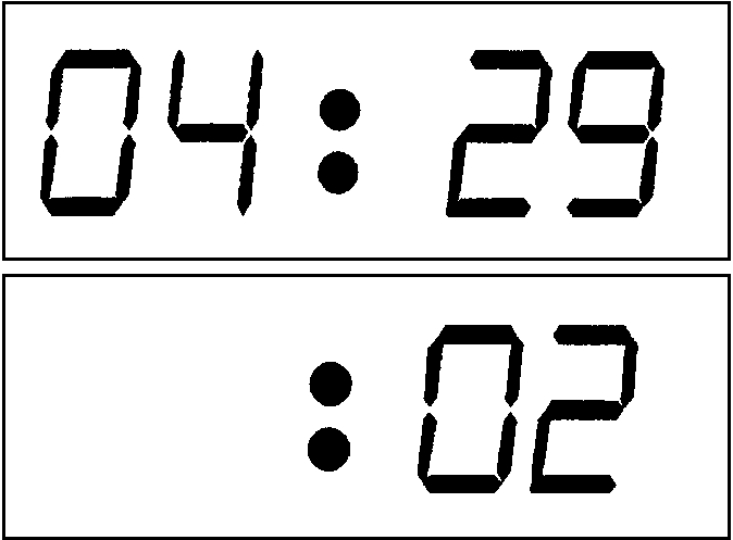
In the case where at least one cycle has been programmed, the display looks like this:
There is an alternation between these two values ??to indicate that the output
is considered active from Monday 3:45. Note that the two central points are
off to clearly indicate that it is an hour's start.


Pressing the NEXT button takes us to the time of arrest. The display changes as follows:
As the time of start-up, there is an alternation between these two values ??to
specify the day and time of decommissioning. The previous example shows a stop
Tuesday at 4:29.


The two central points are fixed to indicate that it is time to stop.
Pressing the CONTINUE key passes on the display of the next cycle.
The two previous steps are repeated until the end of all cycles for the output concerned. Sequence leads to the same stage as already seen for the blank memory.
Return to clock mode is achieved by pressing the button again SUITE.
Editing a time commissioning or stop time of a programmed cycle
The first step to do is to be positioned on the time change.
This is done by pressing NEXT.
When this point is reached, press the UPDATE TIME. Finds the keyboard as defined
in the phase adjustment of the clock.
The hour flashes indicating that it can be changed using the PLUS and reset.
When the correct value is reached, pressing the NEXT passed over the minutes
setting.
These are the minutes flash. The same adjustment operations can be made. Pressing
the CONTINUE key passes on the day setting.
The setting is obtained as for other functions. Pressing the key sequence takes
us back to browse mode.

This phase leads us to a number of comments.
First, in the previous example, this is the time of commissioning that has been modified. This assertion is easily verifiable since the two central points are off.
Then the system is in weekly since it proposes to change the day of service. Indeed, in the daily mode, this step does not exist.
Third, the activation day is Monday for this example (01 days in the position). This cycle thus occurs only once a week. Nothing prevents it to run every day. To do this, simply place the value 00 in day time start.
Finally change the stop time occurs the same way. It only need to be positioned above instead of the time of departure for this report that changing the time of activation does not require any change in the time of arrest.
Return to clock mode requires to be positioned in the end zone programmed.
For this, two methods exist.
The first application to support many times the button NEXT programmed sequences
that are considered for output. This method is used when there is change sequences.
The second fastest application simply press the END key. This button allows
to be positioned directly on the first available memory area.
Return to clock mode only asks one last pressing the NEXT.
Programming an additional cycle set
For this operation, you must select the output to be programmed by pressing the Access button corresponding output x.
It is then necessary to position itself on the first available memory location. For this, the END key can get there right away.
If the display is blank memory (unsaturated), pressing the key Set the time to switch the programming phase of a new cycle.
Playing with the reset buttons, MORE, MORE and it remains to be settled
- The time of starting

- The moment of starting
- The date of start

- Stop time
- Stop the minute
- Day off
This last step is that if the daily mode has not been selected when programming the day started.
The next step leads either to the blank screen, or the memory is full.
A new cycle can then be programmed by pressing the update time or return to clock mode by pressing NEXT.
Deleting a programmed cycle
To do this, we must, as in the case of modification of a cycle to be positioned on the value to delete. Pressing the reset button removes the memory cycle.
Note that the effect is the same positioning themselves on either the departure time or the stop time.
The display returns to viewing the next cycle.
Key actions combined
All the steps that have been seen so far used only one button. The effect of a new could come into action if the previous one had been released before.
However, there are two cases where simultaneous action is needed. The keyboard takes as a function:
The buttons shown in black are those that must be held down to enable this kind
of operation.
Erase all programmed cycles on output
Assigning a new output function is perfectly conceivable quickly.
Erasing all programming for output quickly becomes tedious when there are many.
A quicker solution is to delete all of a sudden
To do so, simply press the button simultaneously on the output and press the
"Reset". When processing is complete, the display shows the number
of the output has been processed. Return to standby mode occurs at the time
of release of the keyboard (the keys are released and reset output).
Note: This function can only be accessed by starting the standby mode (clock).
Do not release the button on the output before pressing the reset button. If
the button was released, the system would go into phase visualization and reset
would be impossible without making a return to the standby mode.
Use of forced mode
It can happen at any time of having to set up an appliance independently programmed cycles. Cela revient à commander manuellement la mise en service de la sortie considérée.
L'activation forcée s'obtient en appuyant simultanément sur la touche relative à la sortie considérée et sur la touche "SUITE".
L'utilisation de cette fonction ne peut s'opérer qu'en partant du mode d'attente.
Le fonctionnement du mode forcé est prioritaire sur le mode programmé. A partir de ce moment, la sortie est activée et le restera quelque soit l'état de commande imposé par la programmation.
Le principe de travail du mode forcé est équivalent à un fonctionnement en bistable. Pour le supprimer, il suffit d'appuyer à nouveau simultanément sur les deux touches qui ont activé ce mode forcé.
Tout comme pour le mode d'effacement généralisé, le système visualise le numéro de la sortie qui vient d'être traitée. Le retour au mode d'attente est obtenu au moment du relâchement des deux touches.
Le mode horaire
Pour le mode horaire, les choses se compliquent un tout petit peu. Le passage du mode hebdomadaire au mode journalier s'effectuait simplement en annulant la valeur du jour dans l'horloge. Sept jours et une valeur pour journalier, cela fait 8. Et sur trois bits, il n'y a plus de place.
Il faut donc se résigner à prendre son fer à souder et opérer une liaison entre la patte 1 (masse ou Vss) et la patte 2 (Int) du 68705.
Cette liaison peut être faite par un simple pont de soudure (si l'utilisation en programmateur horaire est définitive) ou par un cavalier et deux picots qui auront été placés entre le 68705 et l'ULN2003 (Il ya la place et la masse a le bon goût de se trouver là). La liaison entre la patte 2 peut s'effectuer. Cela évite d'avoir à retirer un nouveau circuit imprimé.
Tout ce qui a été expliqué jusqu'ici reste totalement valable sauf pour la partie programmée où il faut remplacer le mot heure par minute et le mot minute par seconde, les fonctions jours ayant tout naturellement disparues.
La notion de jour a cependant été conservée pour la partie horloge à titre indicatif.
Attention les valeurs mémorisées en mode horaire sont totalement incompatibles avec celle du mode hebdomadaire. Le passage de l'un à l'autre impose un effacement général des 4 sorties et une nouvelle programmation.
![]()
The binary file of the MC68705P3 is given in the file uniprog2.bin (2Kb )

![]()
![]() PCB carte affichage Led 7 segments (PDF)
PCB carte affichage Led 7 segments (PDF)
![]() PCB carte affichage LCD (PDF)
PCB carte affichage LCD (PDF)
![]() PCB imprimé carte mère (PDF)
PCB imprimé carte mère (PDF)
![]() PCB clavier (PDF)
PCB clavier (PDF)
![]()

![]()
![]() back to MC6805 MC68705 projects info page
back to MC6805 MC68705 projects info page
![]()
![]() 20 août, 2021
20 août, 2021