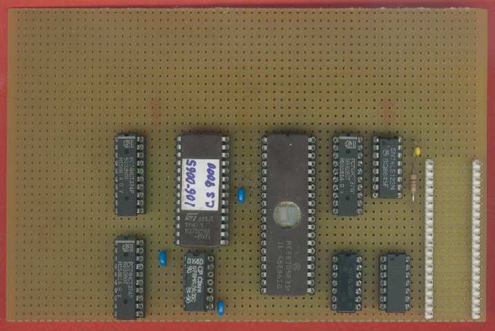
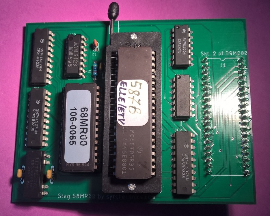
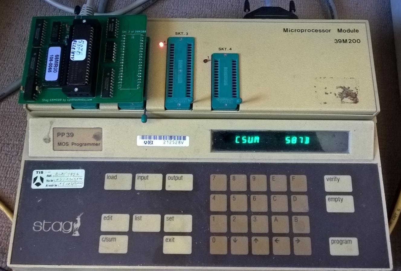
Adapter 68MR00 for Stag PP39 programmer w/ 39M200 Microcontroller
Module
This adapter, to be used with a STAG PP39 /
Zm2500 programmer and a Microcontroller 39M200 Gang Module, allows you the
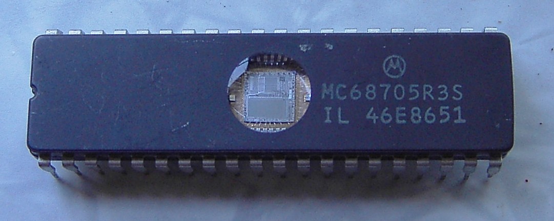
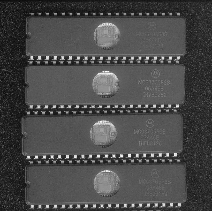
reading of Motorola microcontrollers MC68705R3 and MC68705U3 in less than
1 second. Code can be saved by transfering the binary dump through the serial
line of the programmer using Stag Com1 software.
Note: The 68MR00 adapter can also be used with the Zm2500 Stag programmer.
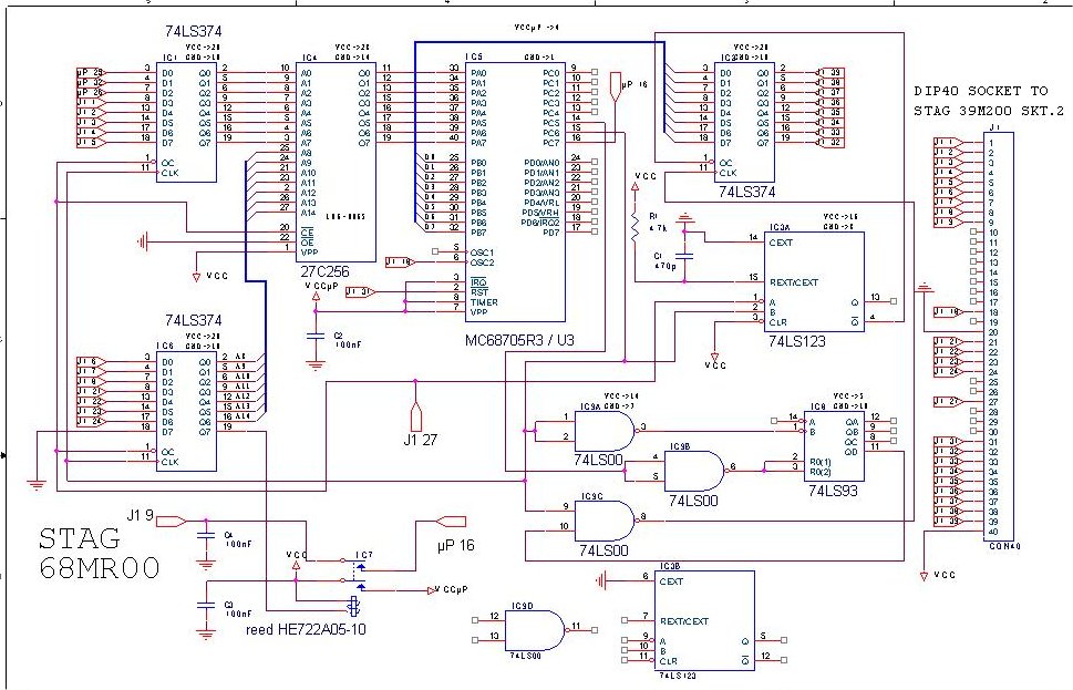
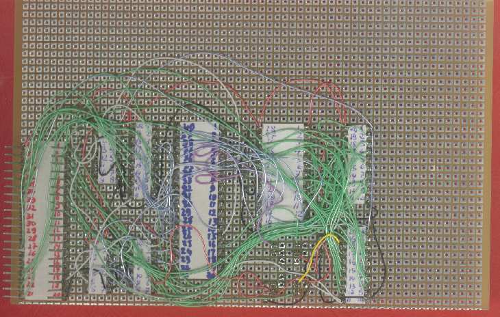
See the Schematic to realize this adapter (pdf printable
format).
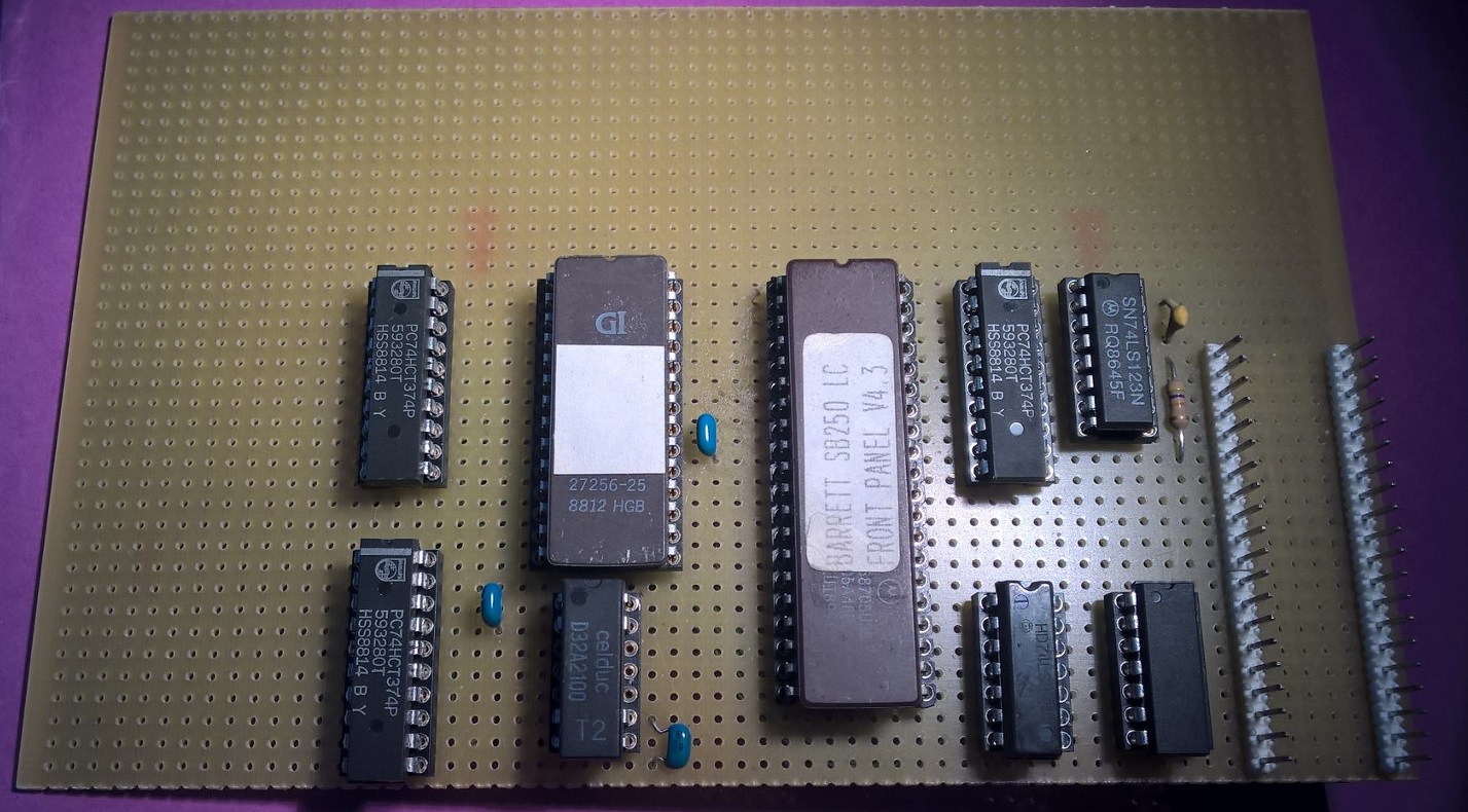
See the content of the EPROM 27C256 106-0065 (checksum 9000) 106-0065.BIN
(32Kb - Shift Click to download)
See Documentation how to use this adapter : This adapter
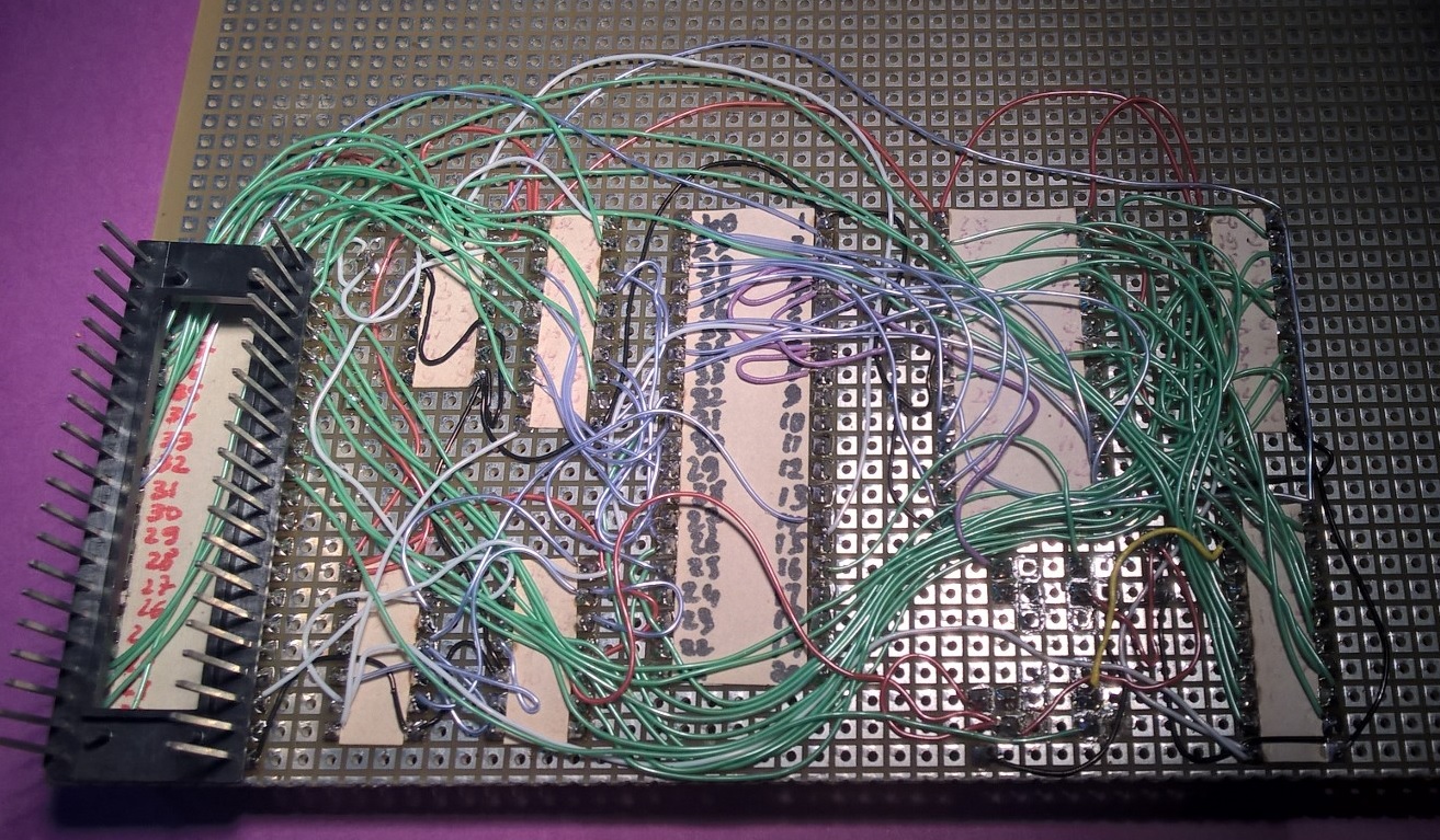
has to be plugged on the SKT.2 DIP40 Socket of the 39M200 Microprocessor Module.
(See on page 4)
******
If you look forward for other information about this 68MR00 Adapter,
do not hesitate to contact me by e-mail at: matthieu.benoit@free.fr
. Also if you have any data about this adapter, read-out method, etc.., do not
hesitate to contribute to this page.
Si vous recherchez des informations pour cet adaptateur de lecture
68MR00, vous pouvez me contacter par e-mail :
matthieu.benoit@free.fr . De même si vous avez des informations sur
la méthode de lecture de cette adaptateur, etc.., n'hésitez pas
à contribuer à cette page.
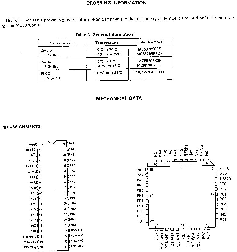
MC68705R3 Pinout useful in order to read the plcc package (MC68705R3CFN):
The 68MR00 is interesting and having more info about the 39M200 would be more helpful since I can only guess what is happening around its socket 2.


There's some strange things too with the 68MR00:
1. there must be a special voltage applied to the uP pin 16
   since it is switched by the relay. It comes from pin 9 of
   socket 2 (called J1 in the 68MR00 schematic). I'm guessing
   it might be the voltage which puts the U3/R3 into its NUM mode.


2. The EPROM address is latched by IC1. But the lower 3 bits are
   unusual. They come from PB0, PB7 and PB1 on the uP. What a strange
   way to do it!!!
   I understand a bit why they control those 3 bits from the uP
   because when you look at the code in the EPROM (IC4) it's
   organised in 8 byte sections:
   C6 00 00 BC 00 00 00 00
   C6 00 01 BC 00 00 00 00
   .... etc to
   C6 0F FF BC 00 00 00 00


   where
   C6 xx xx  is lda xxxx       ie load from memory address xxxxH
   BC 00     is jmp 0000       ie jump back to the start of EPROM
   00 00 00                    I don't think does anything even though
                               it is a valid code (brset)


   Very strange!!
   I think they execute 8 bits of code each then 39M200 changes
   the high address bits and they do it again, etc until all of the
   internal EPROM has been examined. What I don't see is where it
   writes the internal EPROM data to PortB but maybe that has something
   to do with how NUM mode works.


3. uP pins 2 (RST) and 6 (OSC2) are also controlled from socket 2.
   Probably just to provide a clock and a reset signal.


4. uP pins 14 & 15 control the latching of address/data into 8 bit
   latches (IC1, IC2 & IC6). This must be part of NUM.
 Retour au sommaire