MOS Programmer PP39 Stag Programmateur MOS EPROM-EEPROM-µC
Stag PP39
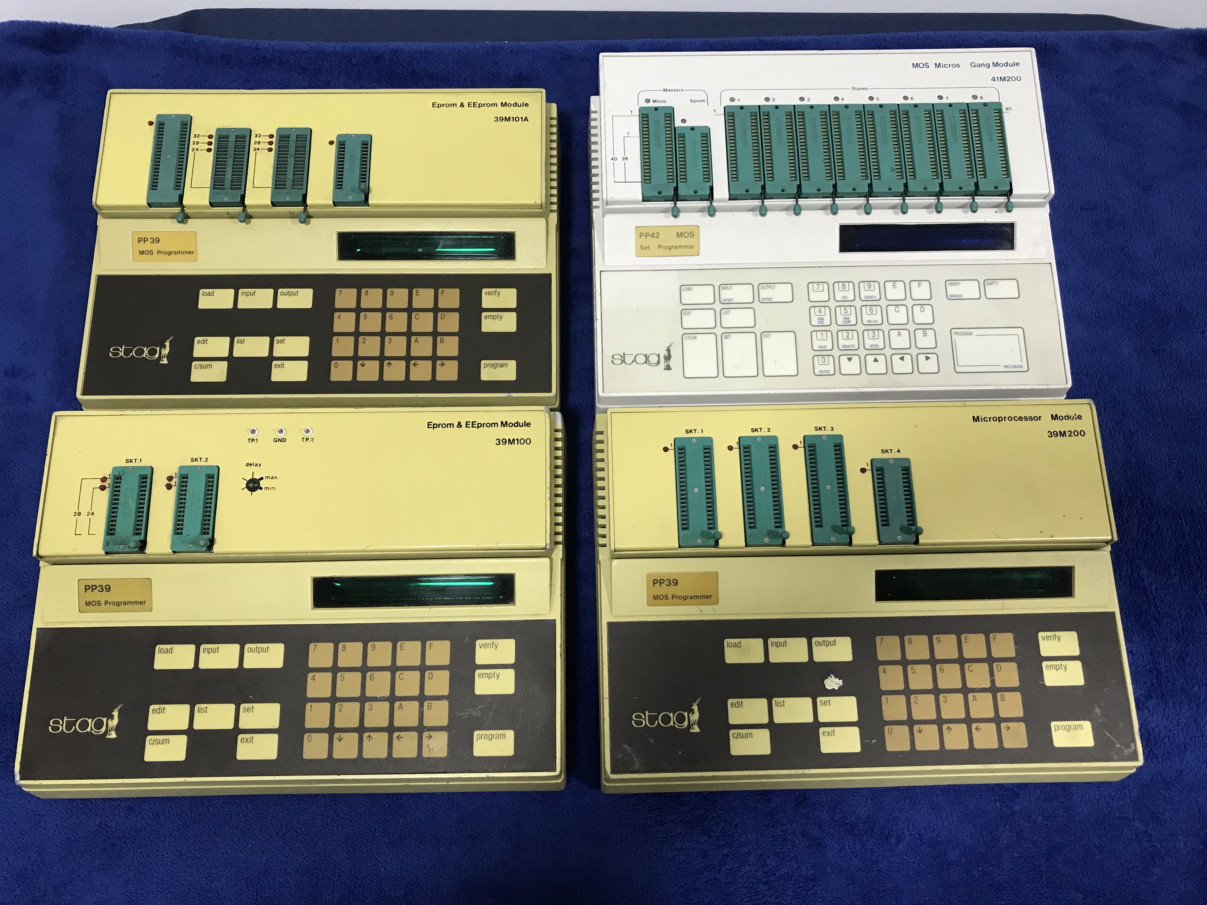
pp39 resources page
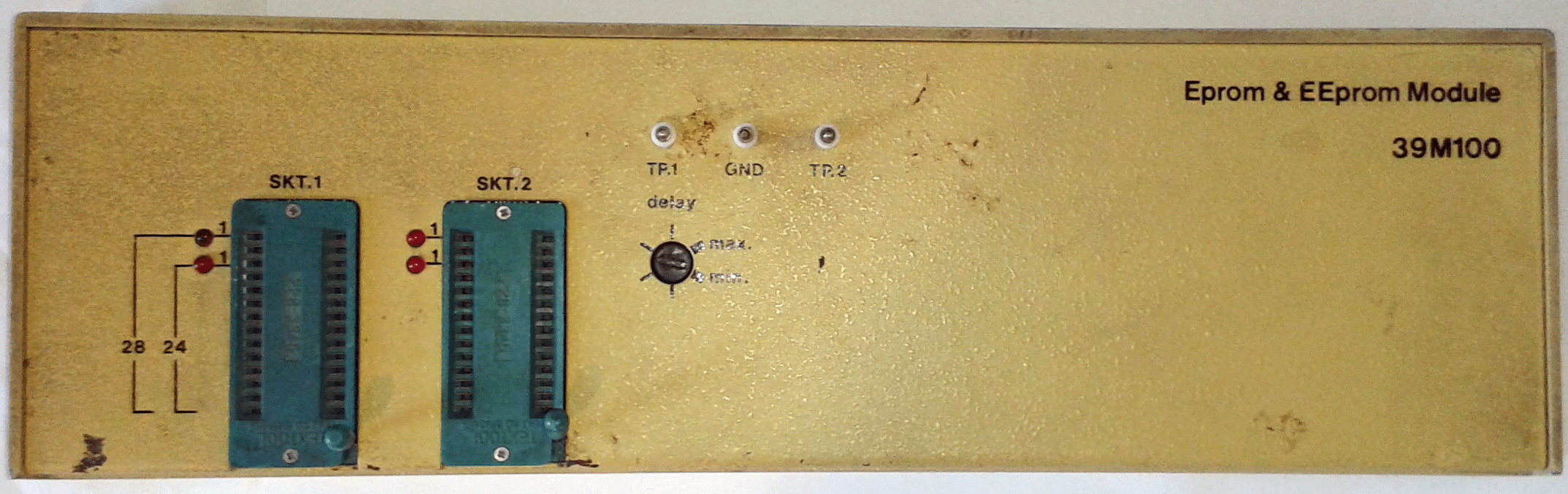
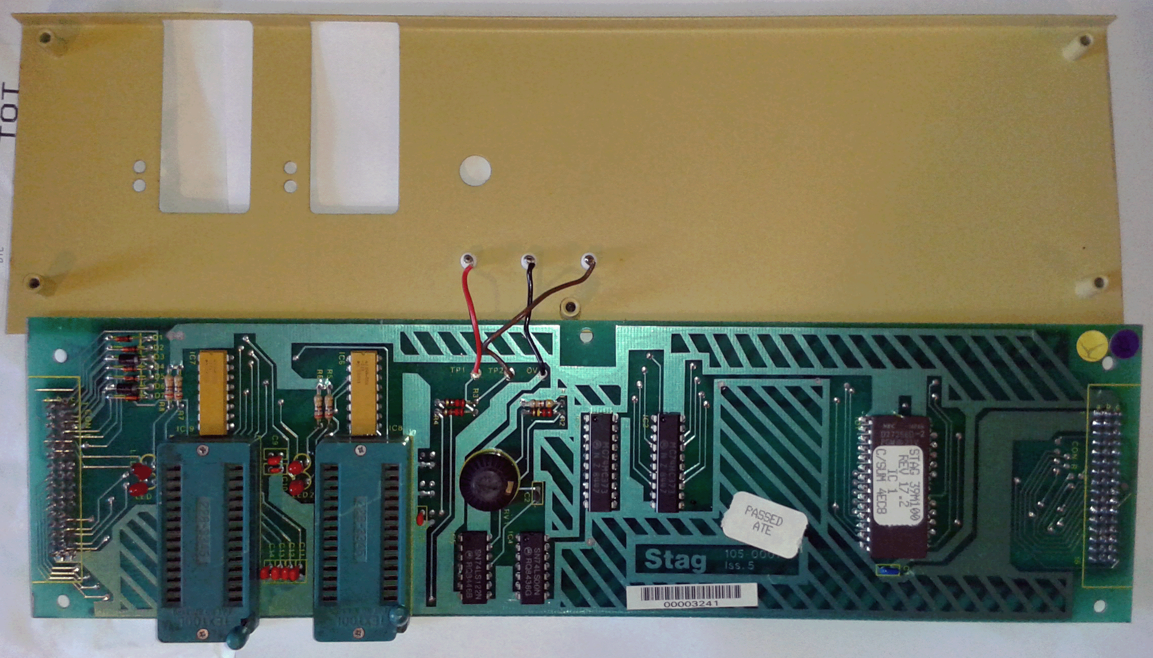
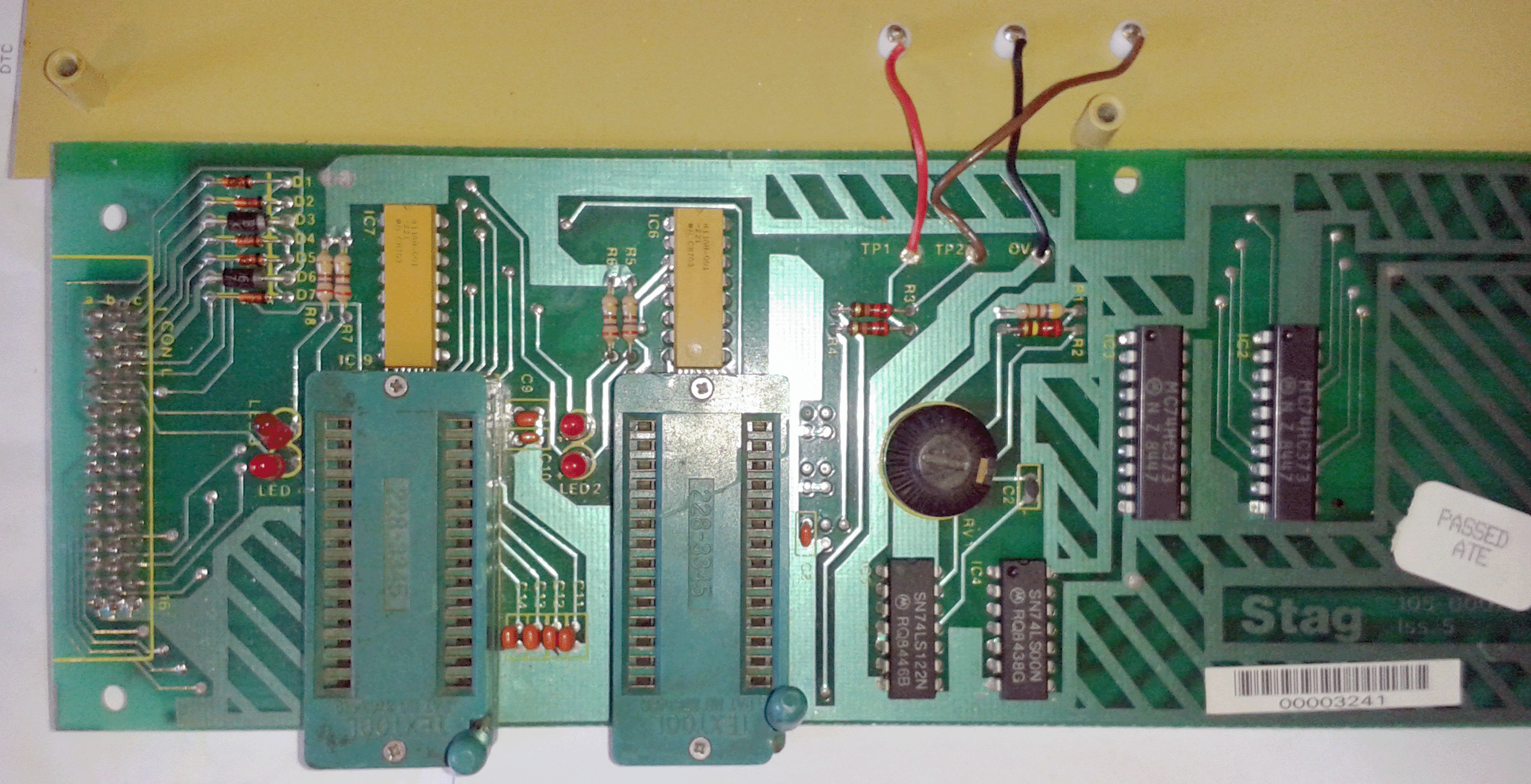
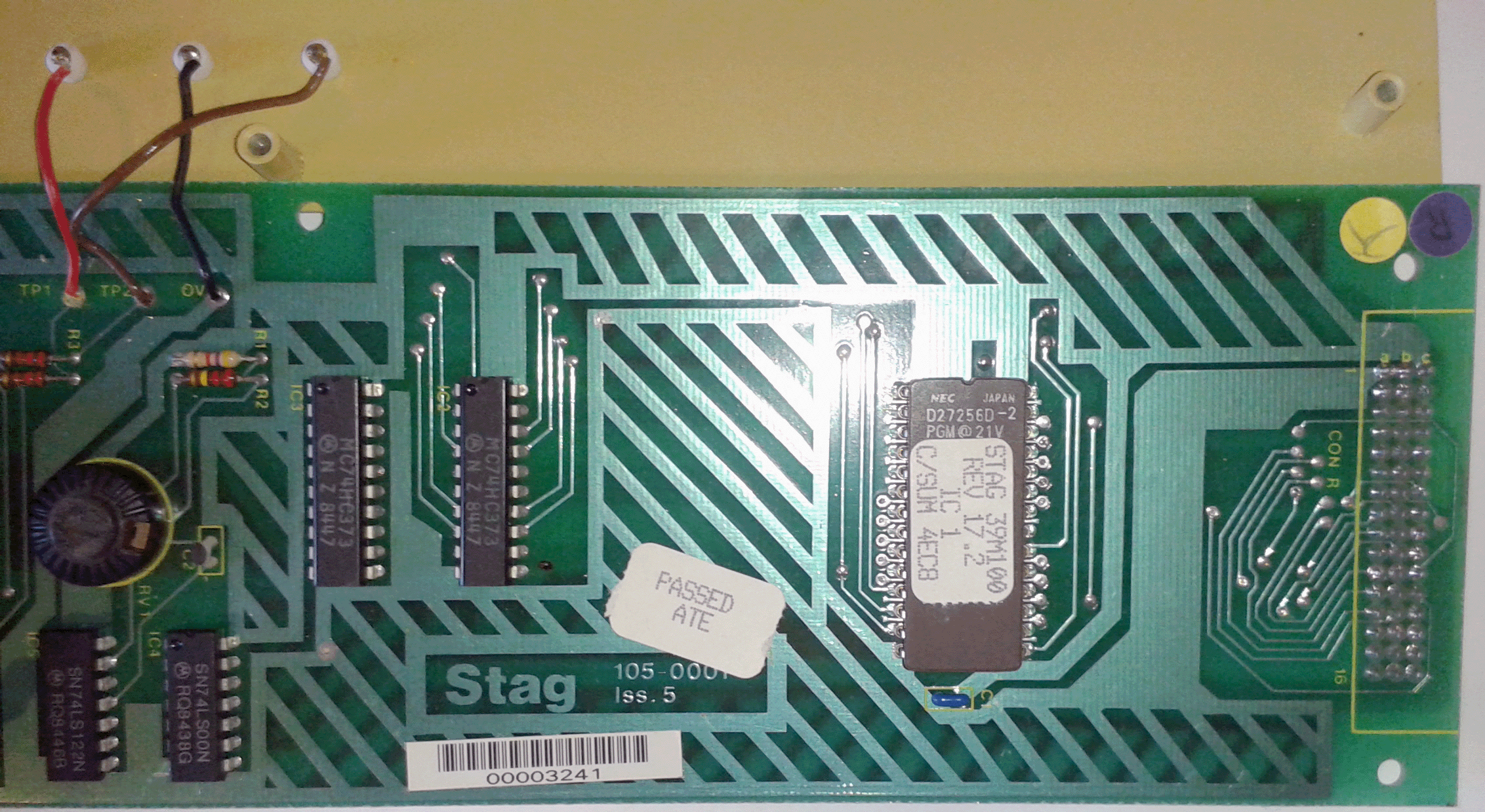
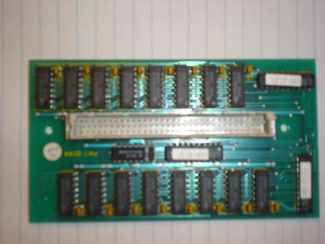
39M101A Eprom&EEprom Module
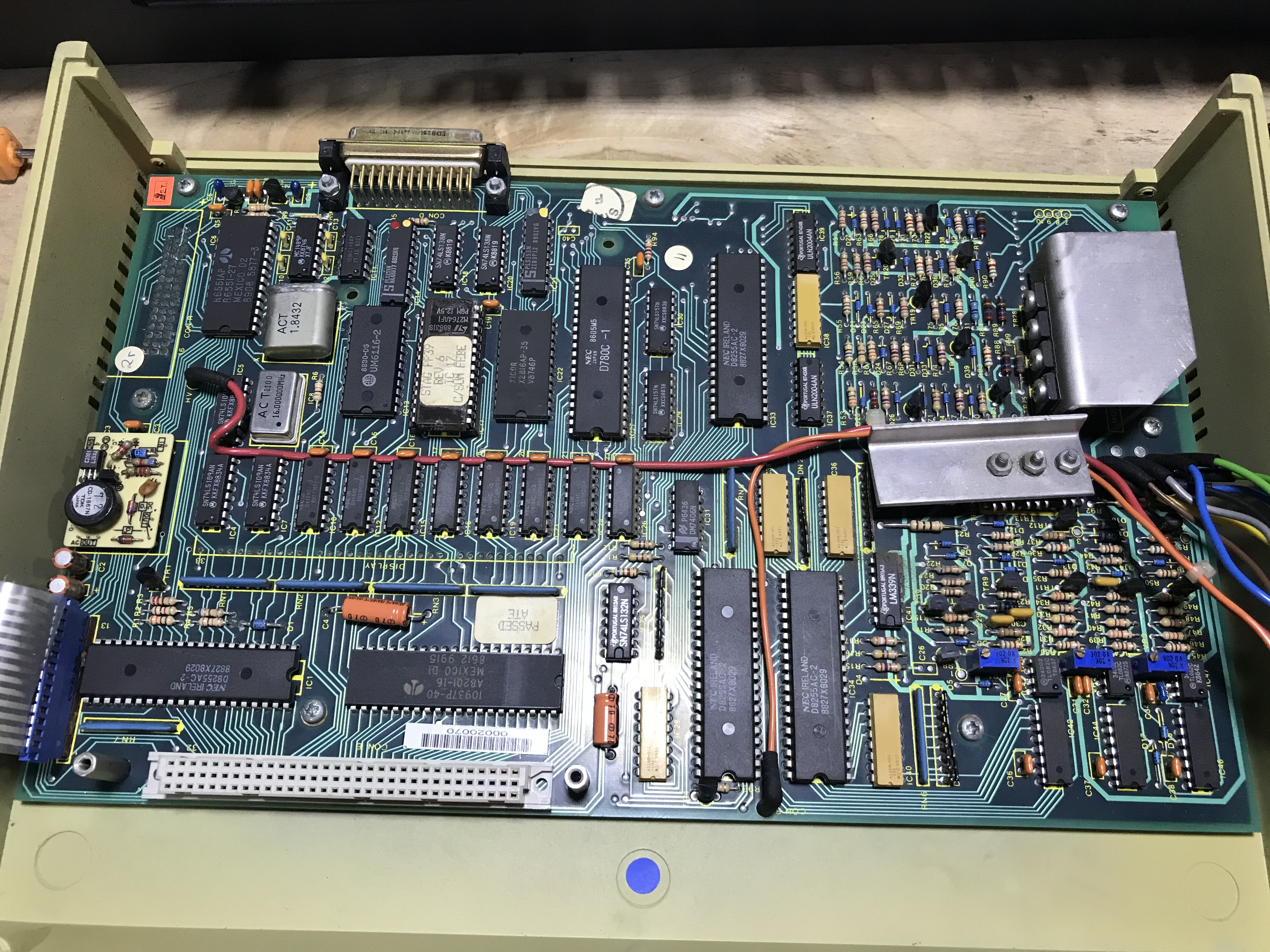
The PP39 is a Universal MOS Programmer, which in conjunction with its family of modules is capable of supporting all MOS erasable PROM
and MICRO devices in NMOS and CMOS technology. The Programmer is software controlled using a single level module approach. This ensures flexibility
and ease of upgrade for future devices whereby the module alone can be returned for software upgrades. (For urgent programming needs a module exchange plan
is available). The PP39 can be operated in ‘LOCAL’ mode or it can be linked to a computer via the serial RS232C interface port enabling ‘REMOTE’
operation of the machine.
FEATURES :
Programming Support: 39M100 Module supports 24 and 28 pin EPROMs
and EEPROMs.
39M200 Module supports 40 pin Microprocessors.
User RAM: 64K x 8 (512 bits)
Expansion RAM to standard 1M bits and 2M bits
Keyboard: 16 Hexadecimal keys, 4 cursor keys and 11 function keys
Display: 16 character alpha numeric green vacuum fluorescent display
Auto Recall: Up to 9 complete machine configurations may be stored in non
volatile memory and recalled at any time. Parameters include device type,
I/O format, RS232C baud rate, address range etc.
Zif Socket Test: Tests zif socket for poor connections or faulty device.
Device Test: Empty, Verify and Illegal Bit
Access Time Test: Variable access time test 100-600ns
Programming Speed: High speed programming algorithms are used where applicable.
Auto Select: The 39M100 module supports Silicon Signature* and Inteligent
Identifier* coded devices. (Revision 2) 15.2-01
I/O Interface: RS232C with full handshake XON/XOFF, device control on input,
keyboard entry of parameters and transmission rates up to 19,200 baud.
Full remote control.
I/O Formats: Supports all commonly used I/O formats including extended formats,
e.g. Intel-hex, Tekhex,
Extended Tek-hex, Motorola S-record, Hex-ASCII, Stag-hex, Binary, DEC Binary
and Binary Rubout.
Audible Alarm: Software selectable to indicate end of program test or as a
warning.
Set Programming: Will program two devices simultaneously with different data
for 16 bit applications. The machine is also configured to program 32 bit
sets.
Edit Functions: String Search, Insert, Delete, Block move, Complement, Interlace,
Fill RAM with test pattern etc.
Self-Test: Automatically runs self-test program on power-up.
Operating Voltages: 100-130V 200-260V 60/50Hz Power Consumption: 70 Watts
update StagView 1.7.2 : story: : with a 39M101A module rev 3.1
and a more modern Linux distribution which would not run the Linux version
of StagView because of changes to one of the libraries it uses.
took some time modifying the code to compile it with the later version of
the tvision library that it requires. When I had something that he could try
I sent it to him and found that the firmware was so old that it had a different
format for the revision number and StagView thought it was revision 0.3 and
no devices could be selected !
added code for the new revision number format and ran my tests
to find the devices supported by rev 3.1.
also found more errors in the module .DAT files which have been there for
20 years or more.
StagView new release can perform checking of the file selected
for "Load from File" to see if it is of the correct type.
It only checks the start of the file but it should prevent the program and
the programmer from locking up if the wrong file is selected.
there is also now the "Disconnect" option which may be useful when
there is more than one programmer connected to a PC.
The other changes were to detect the parallel port type when used on MS-DOS
to prevent lockups if the type if configured incorrectly.
StagView allows the display of up to 10 ports available for
use in the Connect dialog, including USB serial devices for Linux which were
difficult to use before. There is a logging option in Options/other for anyone
interested in the data sent and received; the software has been tested with
USB serial cables.
This new version of StagView fixes some user interface issues
and the "Programmer" menu which is no longer needed is removed.
The device selection dialog also displays if a device entry is supported by
the programmer or is an alias of another device. Stag added other device types
to the .DAT files with identical device codes and those devices are shown
as aliases of the first device in the .DAT file with that code
StagView, 1.6.3 corrects a problem detecting the firmware revision
with 39M200 rev 14.0 and others using 5 digit device codes.
The problem was introduced in 1.6.1 when I added support for rev 2.0. The
result was 4 digit device codes were used for rev 14.0 instead of 5 digit
device codes and no device could be selected
.
http://baddinsbits.altervista.org/bbboot.html
Baddin's Bits Boot disk A FreeDOS boot disk, for CDROM or USB stick, containing
programs capable of communicating with Stag/ GP/ Elan device programmers and
able to use serial and parallel ports on PCI or PCIe expansion cards. Coming
soon.
http://baddinsbits.altervista.org/testfirm.html
Device programmer test firmware Stag PP38/39, Stag PP40/41/42, GP Industrial
Electronics XP640 ; pp3xtest v1.4 which hopefully will detect problems that
the standard firmware doesn't. The interface with the display and keypad is
very basic but if it gets that far the programmer is probably working ok.
Archive
release 7.1 (ZIP Archive -130Kb) to be used under Win98 in DOS-mode
and which works ok to transfer the binary data between the PC and the stag
pp39 programmer
Note: all other archives are buggy to transfer the binary data between the
PC and the programmer
Software
Stag COM1 Last Release (8) (1993) 240Kb Shift-Click to Download (includes
39M100, 39M101, 39M200 devices list). I have noticed that this release is really
buggy for tranmitting binary file from programmer to the P.C. Perhaps it is
depending on the firmware revision of the base unit ?
Stag Software (792Kb - Shift-Click to dowload)
or download the 3 commercial brochures in the Other.zip
archive ( 1.02Mb)
* To Enter Serial Port Configuration : Press SET 1 then with the arrow keys configure as so for example: BIN 19K2 8 1 --
* To go into Remote Mode: Press SET 2 SET (Note to come out from the remote mode : hold on the Exit key while powering up the programmer)
* To See how much memory you have on your programmer, just press SET 4 ; then if it displays 10000 you have 64Kbyte memory and can program eprom until 27C512
if it displays 20000 then you can program eprom of 128 Kbyte i.e. 27C010 for example ; If it displays 80000 then it means you have a 4Mbit memory expansion
board plugged in inside the programmer on the connector DIN41612 32 pins. See below to have the description of this memory card ( 4 Mbit is the maximum capacity
of the stag pp39.)
Notice: when you select the module you use : 39M101 for example make sure the
memory size configurated is the same as on your programmer
for example 10000 if you have no memory expansion, 80000 if you have a memory expansion plugged.
* To see the revision of your module and its description , just press SET 6
* Cable to realize : XON-XOFF configuration :
Sub-D9F(PC)
Sub-D 25M (Stag)
2
- 2
3
- 3
5
- 7
On the P.C. unpack the PP39.ZIP file into a directory called pp39 for example and launch the scom.exe program (this is a DOS Mode Software)
Press ALT-S and select Port Parameters to COM1, 19200 Bauds, Parity None 8 bits, 1 Stop Bit for example.
Then you must see Link to programmer established and Unrecognised command Then Select ALT-P , Programmer PP39
with module M101A for example.
Then select the device, etc.
Eprom BIN files for module 39M101A
Note that revision level 9.0 is not the last release : the latest revision
level for the 39M101A module is 18.4 (dated 1993).
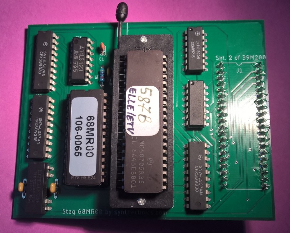
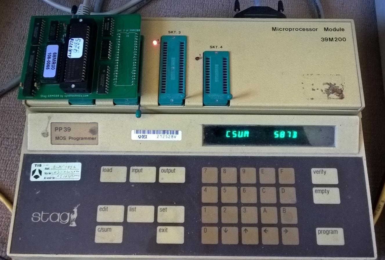
68MR00 : See the description of the 68MR00 adapter
to plug on SKT.2 of 39M200 Module in order to Read Motorola MC68705U3 and MC68705R3:
available everything you need to realize this adapter.
This programmer is interesting . You can fix on the 39M200 module
the adapter 68MR00 to read the MC68705R3
/ MC68705U3 MOTOROLA NMOS Microcontroller. This chip is read in less that one
second with this module by emulating the device.. This module contains an EPROM
firmware to operate the emulation; it uses NUM mode, which stood for Non-User
mode. It was proprietary technique something weird like putting +9 volts on
port C7.
See documentation on last page of the 39M200 Device Support list here
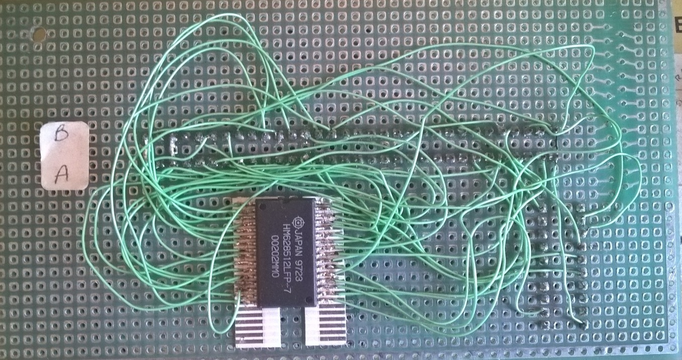
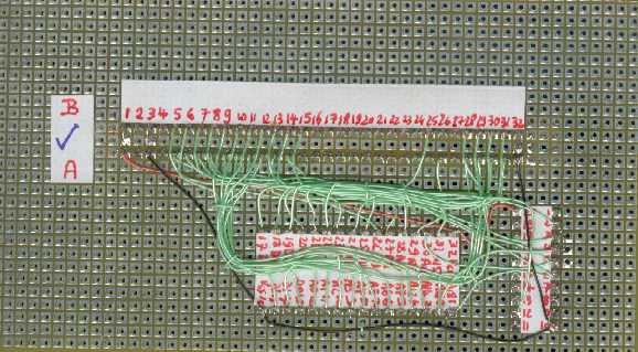
4 Mbit Memory Expansion board for the Stag PP39
Programmer with a 39M101A module, allowing to program from 27C010 to 27C040
Eproms.
Thus the 4Mbits Expansion board for this programmer is no longer available from
Stag UK, a new expansion board based on 512KBytes SRAM ( you can use for example
Hitachi HM628512 70nS Access Time
is OK or Renesas (Mitsubishi) M5M5408BFP
) has been redesigned by Adrian Godwin, using a small PALCE16V8H
for the address decode.
Provides memory decode on an expansion board for the Stag PP39. The 512Kbyte SRAM is located over several pages, at 0x4000 in the CPU memory map. The page
is indexed by LA16-18, and page 0 is provided by onboard memory so is not enabled. Only the CS decode is used in the present system - RD and WR are provided directly
from the CPU.
Wiring
------
I have wired all the address and data lines to their expected points, but this is quite unnecessary - if you make a PCB, the layout may be easier if you order
addresses and data differently.
Connector pin Signal name PAL pin RAM pin Signal name
In general, it seems fairly simple - I expected the PLSs on the board to provide memory size information,
but that doesn't appear to be the case as far as I can see. It looks as though the expansion bus provides
for direct expansion of the multiplexed DRAM interface on the main board, but can also present a non-multiplexed
address bus (and this is what's used by the expansion card I have - the address bus is remultiplexed by the
PLSs on the card.)
I originally traced out all the interconnections between components on the expansion card, that looked at the
signals on the connector to try to work out the functions. I was then going to examine the inputs and outputs
of the PLSs, to work out their programming. This may be difficult, as the outputs can also be inputs - but in fact,
it seems unnecessary as I now believe the expansion can best be done by simply adding memory (e.g. a 4Mbit static RAM)
to the bus with a minimum amount of decoding.
You will notice that there are some address lines that exist as both 'A' lines and 'LA' lines.
The LA lines are latched, probably driven by an I/O port. The memory itself seems to exist in a 16K block of the Z80
address space, from 4000 to 7FFF. So A14 is always '1' when accessing DRAM and A15 always '0'
Therefore, the next address lines used are LA14 and LA15 : the lines used to select 64K banks are LA16 upwards.
When the motherboard DRAM is used, LA16 etc. are all zero but LA16 is 1 when 64K on my expansion board is addressed.
LA16 is 1 when the 64K on my expansion board is addressed. LA17 is briefly used during power-up - I think this is the
memory sizing in action. I'm guessing that the signal on pin a14 is LA18 but it's never active on my system so I can't be sure.
I think a memory board should be built that enables memory in region 4000-7FFF of Z80 addresses, but not when LA16-18 are 0.
MREQ should probably be used to qualif this too, and I may yet find that some of the 'unknown' signals are important.
It's possible that this could be made simpler by disabling the motherboard RAM - perhaps by cutting  the CAS lines to those
devices. It would then be possible to connect the RAM to A0-13, LA14-LA18 and drive chip-select with /(A14./A15./mreq),
i.e. CS is active-low when A14 is high, A15 is low and mreq is low. OE and WR as required.
Eurocard connector to memory expansion module
Several connections are linked directly to the Z80 micro on the main board, and these are mostly used by the memory
expansion board.
A number of connections not used by that board are also available - these are show unmarked below and seem to include
the multiplexed address bus to 64K of motherboard DRAM.

a1 +5
a2
a3 gnd
a4
a5 A15 (Z80 address bus)
a6 A9
a7 A8
a8 A10
a9 A6
a10 A4
a11 A1
a12 A3
a13 LA17 (Extended memory address)
a14 LA18 (perhaps ????)
a15
a16
a17
a18
a19
a20
a21 /rfsh (Z80 output)
a22 /mreq
a23
a24
a25 unknown clock (perhaps raw address enable)
a26 /we (Z80 write signal)
a27
a28 D0 (Z80 data bus)
a29 D2
a30 D4
a31 D6
a32 gnd

b1 +5
b2
b3 gnd
b4
b5 A11 (Z80 address bus)
b6 A12
b7 A13
b8 A14
b9 A7
b10 A5
b11 A0
b12 A2
B13 LA15 (extended memory address)
b14 LA14
b15 LA16
b16
b17
b18
b19
b20
b21 clock (used to drive ras/cas sequencer)
b22 unknown
b23
b24
b25
b26 unknown (perhaps column address enable)
b27
b28 D1 (Z80 data bus)
b29 D3
b30 D5
b31 D7
b32 gnd

a little more detail..
the clock signal on connector b26 is a 2 MHz clock that also drives the Z80 clock input.
Pin a25 is very similar, but is 90 degrees behind - i.e. it rises halfway through the high period of b26
Pin b21 is an 8 MHz clock from which the 2MHz clocks are derived.
b22 is still unknown - It's produced from a PLS on the motherboard and may be related to memory cycles in some way
- perhaps a read select.

Memory tests ?


0000D180 : C1 C9 09 7C A7 28 13 44 ED 42 30 07 09 79 AD E6 : ...|.(.D.B0..y..
0000D190 : 0F AD 4F E1 61 78 C1 47 18 0A 7D E1 C1 06 00 AC : ..O.ax.G..}.....
0000D1A0 : E6 F0 AC 67 2C 2D C0 65 45 C9 20 4E 4F 54 20 41 : ...g,-.eE. NOT A
0000D1B0 : 50 50 4C 49 43 41 42 4C 45 20 20 20 20 20 20 20 : PPLICABLE
0000D1C0 : 20 20 20 20 20 20 20 20 20 20 41 20 48 4F 4C 44 :           A HOLD
0000D1D0 : 53 20 20 20 20 20 20 20 20 20 44 52 41 4D 20 46 : S         DRAM F
0000D1E0 : 41 49 4C 53 20 20 20 20 20 20 44 52 41 4D 20 55 : AILS      DRAM U
0000D1F0 : 4E 44 45 52 20 54 45 53 54 20 20 20 45 58 49 54 : NDER TEST   EXIT
0000D200 : 20 20 20 20 20 20 20 20 20 20 20 20 53 45 54 20 :             SET
0000D210 : 20 20 20 20 20 20 20 20 20 20 20 20 20 20 50 41 :               PA
0000D220 : 53 53 20 20 20 20 20 20 20 20 20 20 20 20 20 20 : SS
0000D230 : 2D 2D 2D 2D 20 20 20 20 20 20 C5 D5 E5 DD E5 FD : ----      ......
0000D240 : E5 11 16 00 ED 73 06 25 2A 06 25 22 FA 23 F6 00 : .....s.%*.%".#..
0000D250 : ED 52 E5 FD E1 F9 AF 32 06 25 32 08 25 21 32 38 : .R.....2.%2.%!28


Calibration ?

0000E550 : E5 8E 64 E6 71 E5 8F 75 E8 9D E5 8B 29 E7 D6 E5 : ..d.q..u....)...
0000E560 : C0 43 ED B7 ED C1 68 ED C3 ED CD 3D E7 D4 ED 01 : .C....h....=....
0000E570 : 20 10 20 20 20 20 20 53 49 4C 53 49 47 20 20 20 :  .     SILSIG
0000E580 : 20 20 10 53 54 41 4E 44 41 52 44 20 50 41 54 54 :   .STANDARD PATT
0000E590 : 45 52 4E 09 43 41 4C 49 42 52 41 54 45 0E 4D 32 : ERN.CALIBRATE.M2
0000E5A0 : 30 30 20 54 52 41 4E 53 46 4F 52 4D 08 4D 4F 44 : 00 TRANSFORM.MOD
0000E5B0 : 20 43 53 55 4D 0B 45 45 50 52 4F 4D 20 42 4F 4F :  CSUM.EEPROM BOO
0000E5C0 : 54 0B 52 4F 4D 20 50 41 47 45 20 4E 4F 08 46 4F : T.ROM PAGE NO.FO
0000E5D0 : 52 43 45 20 51 50 08 42 52 4B 50 4F 49 4E 54 07 : RCE QP.BRKPOINT.
0000E5E0 : 45 4E 41 42 4C 45 20 07 44 49 53 41 42 4C 45 C5 : ENABLE .DISABLE.
0000E5F0 : D5 E5 DD E5 FD E5 21 16 20 4E C5 70 CD 51 CF 0E : ......!. N.p.Q..

A debugger ?

0000E900 : 29 20 20 20 20 20 46 4C 41 47 53 20 20 20 20 20 : )     FLAGS
0000E910 : 20 20 20 20 20 20 46 27 20 20 20 20 20 20 20 20 :       F'
0000E920 : 20 20 20 20 20 20 41 46 3D 20 20 20 20 20 48 4C :       AF=     HL
0000E930 : 3D 20 20 20 20 20 44 45 3D 20 20 20 20 20 42 43 : =     DE=     BC
0000E940 : 3D 20 20 20 20 20 49 58 3D 20 20 20 20 20 49 59 : =     IX=     IY
0000E950 : 3D 20 20 20 20 20 41 46 3D 20 20 20 20 20 41 46 : =     AF=     AF
0000E960 : 27 20 20 20 20 20 48 4C 27 20 20 20 20 20 44 45 : '     HL'     DE
0000E970 : 27 20 20 20 20 20 42 43 27 20 20 20 20 20 53 50 : '     BC'     SP
0000E980 : 3D 20 20 20 20 20 50 43 3D 20 20 20 20 20 41 46 : =     PC=     AF
0000E990 : 27 20 20 20 20 20 03 48 4C 2B 03 44 45 2B 03 42 : '     .HL+.DE+.B
0000E9A0 : 43 2B 03 49 58 2B 03 49 59 2B 03 48 4C 27 03 44 : C+.IX+.IY+.HL'.D
0000E9B0 : 45 27 03 42 43 27 03 53 50 2B 03 50 43 2B 02 4E : E'.BC'.SP+.PC+.N
0000E9C0 : 43 02 20 43 02 4E 5A 02 20 5A 02 20 50 02 20 4D : C. C.NZ. Z. P. M
0000E9D0 : 02 50 4F 02 50 45 F5 3A 9F 24 CB 57 20 0B F1 E3 : .PO.PE.:.$.W ...
0000E9E0 : F5 AF BE 23 20 FC F1 E3 C9 F1 ED 43 86 24 ED 53 : ...# ......C.$.S
0000E9F0 : 84 24 22 82 24 F5 E1 22 80 24 22 8C 24 DD 22 88 : .$".$..".$".$.".


test routine for the PP39
1. press SET
2. press the hidden key between edit and load
3 press A B A
Now you are in the test routine
4. to get back to normal press the hidden key again.
If you look forward for other information about this MOS Programmer,
do not hesitate to contact me by e-mail at: matthieu.benoit@free.fr
. Also if you have any data about this programmer, do not hesitate to contribute
to this page.
Si vous recherchez des informations pour ce programmateur autonome,
vous pouvez me contacter par e-mail :
matthieu.benoit@free.fr . De même si vous avez des informations sur
ce programmateur, n'hésitez pas à contribuer à cette page.


 .
.
 Archive
release 7.1 (ZIP Archive -130Kb) to be used under Win98 in DOS-mode
and which works ok to transfer the binary data between the PC and the stag
pp39 programmer
Archive
release 7.1 (ZIP Archive -130Kb) to be used under Win98 in DOS-mode
and which works ok to transfer the binary data between the PC and the stag
pp39 programmer


 Retour au sommaire
 Retour
à la Page d'accueil
Retour
à la Page d'accueil